
MD has secured patent 12080632 for its innovative glass core substrate technology, poised to replace traditional organic substrates in multi-chipset processors in the years ahead.
While AMD does not directly manufacture semiconductors, it is ahead of rivals like Intel and Samsung, who are also exploring glass substrates for next-gen components. This patent ensures AMD’s freedom to innovate with glass substrates while protecting the company from potential legal challenges and limiting competitors from adopting similar approaches.
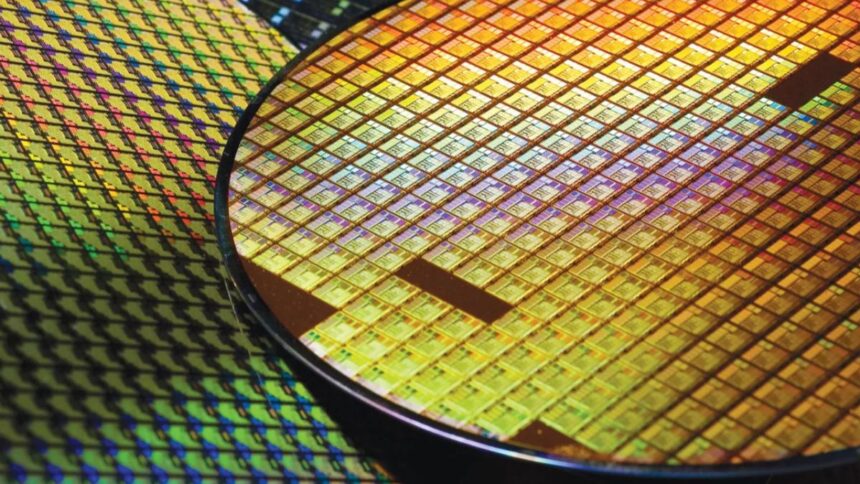
Benefits of Glass Substrate Technology
Switching to glass substrates offers several significant advantages over traditional organic materials:
- Unmatched Flatness: Enables precise alignment for dense interconnects.
- Dimensional Stability: Maintains consistency even under demanding conditions.
- Superior Thermal and Mechanical Strength: Improves durability and reliability for high-performance computing.
These benefits allow AMD to enhance the accuracy of lithography processes, enabling ultra-dense interconnections in advanced system packaging. This innovation will improve the reliability of server processors, particularly for applications involving high temperatures and intensive workloads.
AMD Challenges with Glass Substrates
AMD’s patent reveals that the main hurdle in developing glass core substrates was creating “Through Glass Vias” (TGVs). These vertical pathways within the glass core are essential for transmitting power and data.
Producing TGVs requires advanced techniques like wet etching, laser drilling, and magnetic self-assembly—a newer method still gaining traction.
Despite this shift to glass, AMD will continue to use organic dielectric materials and copper in its designs. These will be applied to one side of the glass wafers, necessitating a fresh approach to redistributing layers in advanced chip packaging processes.
The patent outlines a reliable connection solution by using copper-based bonding instead of traditional soldering. This method ensures strong, vacuum-free connections, eliminating the need for filler materials. As a result, it becomes possible to stack more substrates, enhancing the potential for greater performance and efficiency in chip designs.
AMD’s Glass Substrate Patent Opens Doors to Diverse Applications
AMD’s newly registered patent extends the potential use of glass substrates to various applications, significantly broadening the company’s scope. The patent covers high-density interconnections, which could benefit servers, mobile devices, computer systems, and even advanced sensor technologies.
Though AMD doesn’t manufacture its chips and relies on partners like TSMC for production, the company could still capitalize on the patent in other ways. By licensing this technology to commercial partners, AMD can generate additional revenue streams while fostering innovation across the tech ecosystem.


