
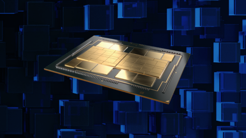
Intel has recently patented a new modular GPU design that uses chiplets—small, independent chips—like “LEGO pieces” to build a scalable graphics processor. This approach, already seen in CPUs but more challenging to implement in GPUs, could enable Intel to build more flexible and powerful GPU configurations, optimize energy management, and potentially reduce production costs. This innovation marks a significant development for Intel, as it moves to diversify its GPU lineup with more adaptable and efficient designs.
The patent, which Intel submitted in September 2023 and had approved in early October, outlines a technology to disaggregate a System on a Chip (SoC) using multiple chiplets. While chipset-based designs have long been used in CPUs, they are rare in GPUs because of the high demands for low latency and intensive data transfer inherent in graphics processing. Only a few AI and data center accelerators, like AMD’s Instinct MI325X, have used a similar approach.
Intel’s design proposal combines logic chiplets (where the GPU’s processing cores are housed) with memory chiplets, all connected via a bridge and a high-speed interconnect system or “fabric” mounted on a base chipset. This modular configuration is similar to what Intel has implemented in its Meteor Lake, Lunar Lake, and upcoming Arrow Lake CPUs, though with additional complexity to handle the needs of a GPU. This new structure could not only expand Intel’s capacity to develop high-performance GPUs. Still, it could also lower barriers to producing more customizable and power-efficient graphics solutions for consumer and enterprise markets.
Intel’s second attempt
Intel had previously experimented with a similar modular chiplet-based architecture in its Data Center GPU Max line, codenamed “Ponte Vecchio.” This high-performance GPU, which Intel discontinued in May, incorporated 16 compute chiplets, four high-bandwidth memory (HBM) modules, and over a dozen high-speed communication chiplets, all within a single package. This design approach closely resembles the concept outlined in Intel’s newly registered patent.
The modular chiplet strategy offers several benefits. By assembling GPUs from smaller chiplets, Intel can create scalable configurations with lower manufacturing costs. This flexibility also allows dynamic control of each chiplet, improving power efficiency and enabling finer control over power consumption. However, a key challenge with this architecture is the slight performance latency introduced by the spaces between chiplets—an issue Intel addresses with its high-speed interconnect “fabric,” which reduces delays.
Intel’s recent patent filing suggests the company is exploring ways to adapt this modular architecture for future products, possibly extending to consumer-oriented GPUs, such as gaming graphics cards. AMD has already experimented with a chiplet approach in its Radeon RX 7900 XTX and 7900 XT GPUs, though only for memory components.
However, for broader use in GPUs, particularly with complex compute elements, it may still be a few years before such architectures become mainstream due to the technical demands of integrating multiple high-performance chiplets.


