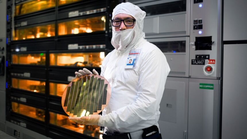
Despite rumors suggesting setbacks in Intel’s 18A lithography process, the company has confirmed that development is progressing well. During a conference this week, Intel stated that it has successfully implemented SRAM with the same density as TSMC’s N2 process, directly contradicting previous speculation.
As the world’s largest semiconductor manufacturer, TSMC holds key clients and leads in technological advancements. However, Intel’s latest update marks a major step forward for Intel Foundry, strengthening its push toward semiconductor independence and attracting more customers.
Another key development in this new era of chip manufacturing is Intel’s Backside Power Delivery Network (BSPDN)—a groundbreaking power delivery system routed through the back of the silicon. If successfully implemented, it would be an industry first, with the upcoming Panther Lake architecture potentially being the first to feature this innovation.
Advance can yield faster CPUs
With the Intel 18A process, Intel aims to achieve an SRAM density of 38 MB/nm², matching the 38 MB/nm² promised by TSMC’s 2nm lithography. TSMC has also revealed that its SRAM cells will measure 0.175 µm²—a key factor since smaller cells allow for higher memory capacity within a compact space.
Advancements in SRAM manufacturing are crucial, as this technology is widely used in cache memory and other hardware components. Higher-density SRAM enables processors to have larger caches, leading to better performance and efficiency.

