
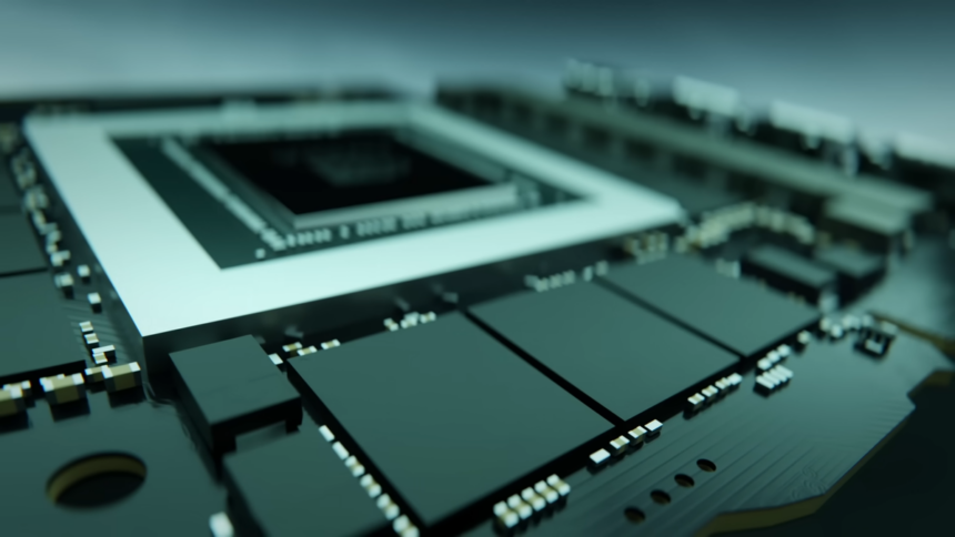
At the same conference where Intel Foundry shared updates on chip manufacturing, NVIDIA also unveiled its plans. The company is working on AI accelerator GPUs that utilize 3D packaging technology featuring vertically stacked tiles.
This approach will replace traditional electrical interposers with advanced photonic silicon (SiPh) interposers. By stacking tiles vertically, NVIDIA’s design will allow up to four GPU tiles per “tier,” each tile incorporating 12 SiPh connections.
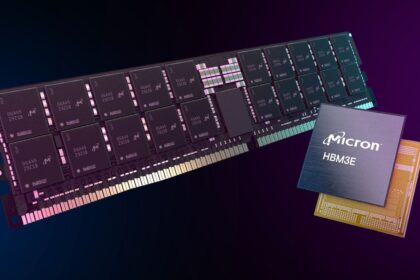
In addition, NVIDIA is developing stacked DRAM within the same packaging, further enhancing performance and efficiency. This innovation reflects the Green Team’s commitment to pushing the boundaries of GPU technology, particularly for AI-focused applications.
Benefits and challenges with NVIDIA innovation
By stacking different dies, NVIDIA aims to reduce communication latency and increase bandwidth, much like AMD’s 3D V-Cache technology used in Ryzen processors. This method could significantly enhance GPU performance, especially for AI applications.
However, bringing this technology to consumers poses significant challenges. For one, NVIDIA would need to manufacture an enormous number of photonic silicon (SiPh) connections each month, a technically demanding task. Additionally, die stacking results in higher chip temperatures, an issue that still requires practical solutions to ensure reliability.
Given these hurdles, the new chip packaging technique is not expected to become commercially available until the decade’s end.
The International Electron Devices Meeting 2024 concludes this Wednesday (11), where industry leaders in technology and semiconductors, including NVIDIA, presented advancements to make chip manufacturing more efficient while delivering greater performance for end users.


