
Samsung is making significant moves to reshape its semiconductor division, focusing on the mass production of 2nm and 1.4nm components, which is critical for its future in the highly competitive chip-making industry. The company is reorganizing its factories in South Korea to accommodate these advanced lithographies, addressing challenges that have plagued its semiconductor sector.
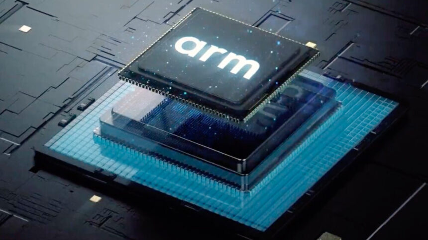
Notably, this shift coincides with the announcement of a partnership with ARM to produce a 2nm AI accelerator, highlighting the strategic importance of these new technologies.
According to Business Korea, Samsung is already setting up equipment for the S3 production line at its Hwaseong plant, which will handle 2nm chip production starting in Q1 2025. The facility aims to produce up to 7,000 monthly wafers at total capacity.
Meanwhile, the Pyeongtaek 2 factory is preparing the S5 line for 1.4nm chips, with production set to begin in Q2 2025, albeit at a smaller scale of 2,000 to 3,000 wafers per month.
Samsung is also repurposing parts of its S3 line that are currently focused on 3nm production to shift toward 2nm, while other factories will continue to focus on memory manufacturing.
The first tests of these cutting-edge manufacturing technologies are linked to the Tethys Project, which is expected to become the Exynos 2600 and power the Galaxy S26 series in 2026. Samsung is also testing chip designs for key clients, including Preferred Networks (Japan), Ambarella (U.S.), and Qualcomm, the maker of Snapdragon processors.
Samsung’s strategic overhaul is driven by two significant factors: the intense competition with TSMC, the world’s leading chip manufacturer, and the company’s internal struggles with maintaining high production standards and securing major clients. These difficulties have negatively impacted Samsung’s financial performance, prompting the company to issue a public apology.
One insider emphasized the importance of the shift to 2nm technology, stating that ensuring its success has become a “matter of life and death,” especially following delays with the Exynos 2500 chip, produced using a 3nm process.
The partnership between Samsung and ARM
Samsung’s recent moves in the semiconductor space are starting to show promise, as evidenced by the newly announced partnership with ARM and ADTechnology and Rebellions to create an advanced artificial intelligence (AI) accelerator. This collaboration will integrate ARM’s Neoverse V3 CSS platform with ADTechnology’s computing chiplet and Rebellions’ AI accelerator into a single package. This package will be manufactured by Samsung using its cutting-edge 2nm process featuring GAAFET transistors.
This partnership aims to develop a solution capable of handling complex generative AI tasks, focusing on applications like cloud computing, high-performance computing (HPC), and general AI/ML workloads. According to the companies’ projections, the new AI accelerator is expected to deliver performance gains of two to three times over traditional CPUs when processing large language models (LLMs), such as the 405 billion parameter version of Meta’s Llama 3.1.
While there’s no exact timeline for mass production, the official launch of this AI accelerator is anticipated for 2025, around the same time that Samsung is expected to begin high-volume 2nm production.
More details about the product and its performance are expected in the coming months. This partnership is a key indicator that Samsung’s strategic efforts in the semiconductor space are beginning to yield positive results, positioning the company competitively in the growing AI market.
Source: BusinessKorea


