
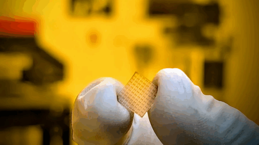
The tech industry thrives on constant innovation, and a recent breakthrough from Stanford University could push chip technology into an entirely new era. Researchers there have successfully developed a new type of power conductor using an incredibly thin 1.5 nm film, achieving results that current conventional manufacturing methods can’t match.
As detailed in a study published in Science magazine, the experiment began by applying a thin layer of niobium onto a sapphire substrate. The team experimented with various thicknesses of this niobium layer—ranging from 4 nm down to just 1.4 nm—representing a 50% reduction in lithography size compared to what’s used in modern AMD and Intel processors.
Next, they coated the niobium with a layer of niobium phosphide, creating a film composed of multiple crystal grains distributed uniformly. This film was tested at thicknesses ranging from 80 nm down to 1.5 nm, with researchers conducting extensive trials to fine-tune the application process and identify the optimal configuration.
Low resistance and great conductivity
The main goal of this research is to achieve exceptionally low electrical resistance, and the results are impressive. At just 1.5 nm, the niobium phosphide layer demonstrated a resistance of around 34 micro-ohms per centimeter at room temperature. That’s roughly six times lower than thicker layers, and far below copper, which is currently the industry standard and offers about 100 micro-ohms per centimeter.
Thanks to this ultra-low resistance, the new film delivers significantly higher conductivity than materials used in today’s semiconductor chips. This means faster and more efficient power delivery at a microscopic scale.
Even more promising is that the process is compatible with existing chip manufacturing technologies, giving it strong potential for real-world adoption. This innovation could play a key role in the next generation of ultra-efficient, high-performance processors if scaled successfully.


