

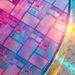
At the International Electron Device Meeting in early December, TSMC shared exciting updates about its progress in chip manufacturing. The company’s upcoming 2nm lithography process promises significant improvements, offering 15% better performance and 35% lower energy consumption compared to current chips.
This leap is partly due to a 1.15x increase in transistor density over the existing N3 (3nm) process. TSMC’s new N2 NanoFlex technology also plays a key role by enabling more cells to fit into smaller spaces, maximizing efficiency and performance.
In addition, TSMC is moving away from traditional FinFET technology to embrace a new design that provides greater control over current flow. This transition ensures better scalability and improved reliability for its customers, setting a new standard for advanced semiconductor manufacturing.
Advancement will cost 10% more than 3 nm node
This technological leap comes with a steep price tag. Companies looking to adopt TSMC’s new 2nm manufacturing process will face a 10% cost increase compared to the current N3 process. Each silicon wafer could range from $25,000 to $30,000, making it up to $10,000 more expensive than wafers produced with the existing technology.
However, it will be a while before the PC hardware industry can utilize chips based on this advanced node. Mass production is slated for the second half of 2025, meaning the first products featuring 2nm technology may not hit the market until 2026.
Despite the costs, TSMC’s 2nm node is drawing interest from major players like NVIDIA, AMD, Apple, and even Intel, despite the latter’s emphasis on its own factories. The promise of higher performance and lower power consumption is a compelling prospect for the entire tech industry.
Source: TSMC


