
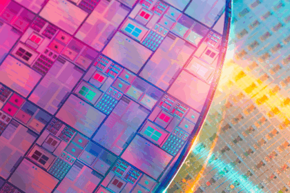
Cache memory, a critical component of processors, utilizes SRAM technology, and advancements in this area are shaping the future of semiconductor manufacturing. According to a document previewing the 2025 International Solid-State Circuits Conference (ISSCC), TSMC’s 2nm (N2) process demonstrates significant refinement compared to Intel’s 18A lithography in terms of SRAM density and cell size.
Key Comparisons: TSMC N2 vs. Intel 18A
- TSMC N2 (2nm):
- SRAM Cell Size: 0.0175 µm².
- Density: 38 Mb/mm².
- Expected to launch in the second half of 2025.
- Intel 18A (1.8nm):
- SRAM Cell Size: 0.0210 µm².
- Density: 31.8 Mb/mm².
- Comparable in refinement to TSMC’s current N3 (3nm) node.
This means that TSMC’s N2 node will offer denser and smaller SRAM cells, packing more memory into the same physical space, which is advantageous for high-performance processors and other applications.
Why SRAM Refinement Matters
Shrinking SRAM cells is a challenging task due to the stability and reliability demands of this technology. However, advancements bring numerous benefits:
- Faster processing speeds due to reduced latency in cache memory.
- Greater capacity in a smaller footprint, optimizing processors for AI, gaming, and mobile devices.
- Applications include not only CPU cache memory but also SSD caches, routers, smartphones, and more.
Future Outlook
The progress in SRAM technology marks a milestone in semiconductor manufacturing, particularly as TSMC edges closer to deploying its N2 node in 2025. As AI chips and other advanced technologies continue to drive demand for high-performance semiconductors, the industry eagerly awaits detailed updates at the ISSCC 2025 in February.
With innovations like these, TSMC is solidifying its leadership in the race for smaller, more efficient nodes, while Intel continues its push to remain competitive in a rapidly evolving landscape.


